FSI & BSI imagers
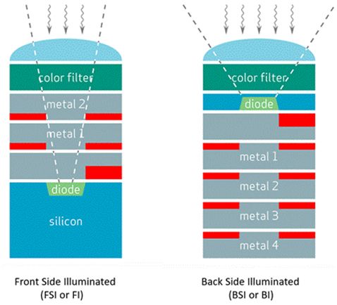
The previous article titled “The Photoelectric Effect in Image Sensors” described the method in which incident photons generate electron-hole pairs, from which the photoelectrons are collected in the depletion region of a pixel. Conventional CMOS imagers are implemented as Front Side Illuminated (FSI) structures, as shown schematically below. In this article, we describe the main differences between FSI imagers and BSI or Back Side Illuminated imagers, which are also shown schematically below for comparison.
In a front-side-illuminated (FSI or FI) imager, gate structures can absorb many of the incident photons, reducing the number of photons that reach the depleted region (the photodiode). This reduces the QE of the device, and can attenuate the response at certain wavelengths, particularly towards the 350~400nm (blue) region of the spectrum. FSI imagers are produced in higher volume than their BSI counterparts. For this reason and because scientific grade BSI imagers are targeted towards light-constrained applications, they typically command a price premium over FSI imagers. Since the light passes through more layers in an FSI imager, the photonics of the device are somewhat different from that of the semiconductor material.

By using microlenses and other techniques such as light pipes QEs of greater than 80% can be achieved with CMOS FSI imagers. Image sensor manufacturers such as Sony also use 3D “stacking” in some of their imagers. This process removes some of circuitry from the photosensitive layer onto one or more layers that are connected by through-silicon vias (TSVs). This increases the die space available for photosensitive pixels, while also allowing for greater on-chip processing capabilities.
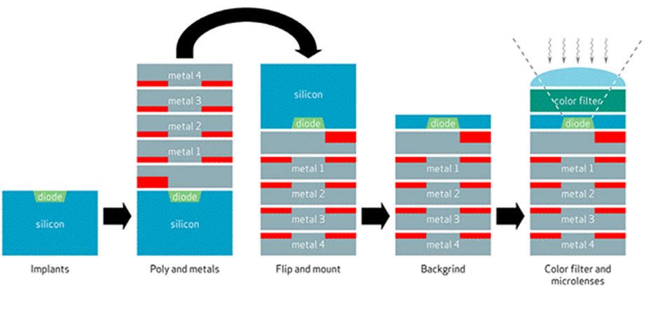
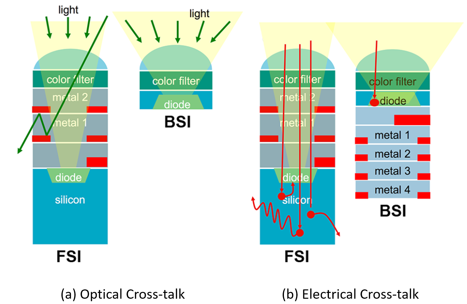
In a back-side-illuminated (BSI or BI) imager, the pixel structure is reversed. This requires an expensive etching/grinding process of thinning the bulk of the silicon until it only a few microns thick and is transparent to light exposing the photodiode more directly to the incident photons. The gate structures are now on the other side of the photodiode, removed from the imaging path. The result is less optical cross-talk, a higher QE (often exceeding 90%), and a spectral response which is closer to that of the semiconductor material. BSI imagers can also capture a wider cone of light which reduces the thickness of the lens array, allowing for wider aperture lenses.

In general, the structure of FSI imagers makes them more prone to cross-talk, both optical and electrical. Optical cross-talk occurs when a photon that is incident on a pixel gets collected by an adjacent pixel. Electrical cross-talk occurs when a photoelectron from one pixel drifts into an adjacent pixel, or into the substrate.

The following table shows a selection of sCMOS cameras with BSI imagers, with their salient specifications:
** Peak QE is shown for monochrome versions of each camera series (see QE Curves in the next article). Max frame rate is displayed as max frame rate at full resolution.
References:

