Spectral signatures are like unique fingerprints for different materials. These signatures, composed of characteristic patterns of light absorption and reflection, can reveal crucial information about the composition and properties of various substances. Even materials that appear the same to our eyes can be identified by their spectral signatures, and this can be used in many applications.
Spectral signatures result from the interaction between electromagnetic radiation (typically light) and a material’s surface. When light interacts with a material, some wavelengths are absorbed, while others are reflected, transmitted, or scattered. This behavior is governed by the material’s chemical composition, structure, and physical properties.
Thus, the light that is collected from a material acts as a messenger – conveying valuable information about the composition, structure and properties of the material. A spectral signature is typically visualized as a graph which displays the intensity of light at different wavelengths that is collected from the material. By analyzing these spectra, we can discern unique patterns that serve as identifiers for specific materials.
For example, one may use the spectral signatures obtained from the leaves of plants to identify whether the plants are healthy.
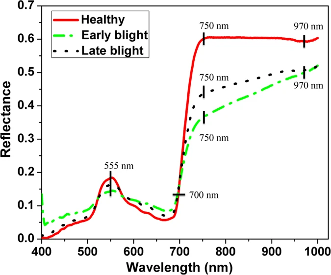
The spectral signatures of healthy, early blight and late-blight diseased leaves of tomato plants are shown below. Since these signatures are of the leaves of the same variety of tomato plants, the general trends of the three spectral curves were quite similar. There is a peak at around 555 nm and a valley at around 680 nm. The peak at 555 nm is the nitrogen absorption band. Reflectance increased sharply with the wavelengths from about 680 to 750 nm. Wavelength at 700 nm is the red edge. From 700 to 1023 nm, the high reflectance was due to the internal light scattering by leaf cells. The reflectance in the visible spectral region is lower than that in the near-infrared region.

It is possible to detect the onset of disease because the reflectance of healthy samples is higher than that of infected ones in the near-infrared region (750–1000 nm), which is caused by the collapse of leaf cell structure as the disease spreads. In the visible region (400–750 nm), there is some overlap between healthy and diseased leaves. The moisture content of healthy samples is higher than that of the diseased ones, resulting in a noticeable dip at 970 nm for healthy samples.
There are numerous use-cases in which the spectral signature of certain materials can be used in identification, classification and sorting. Applications range from remote sensing from airborne or space-based platforms – to handheld devices or laboratory mounted systems for research. Depending on the type of material, the spectral information of interest can be in different parts of the electromagnetic spectrum. In the above example, there is spectrally significant information in the Visible-NearInfrared (VNIR or VISNIR) region from 400-1000nm. In a different use-case, e.g. in sorting fabrics for recycling (based on their material, not on their color) the spectral information of interest may be at higher wavelengths [900-1700nm].
It is important to choose an image sensor which is sensitive to the range of wavelengths that are convey spectrally significant information in a given application.
Image Sensors
The Knowledge Base article titled “C3) The Photoelectric Effect in Image Sensors” describes the process by which incident photons of certain wavelengths generate photoelectrons in certain materials based on the bandgap energy (Eg) of the material. As was detailed in that article, the bandgap energy of Silicon [Eg = 1.12eV] sets the upper end of its range at 1110nm. This means that Silicon-based image sensors are useful in the Ultraviolet and Visible range. They are also useable in the Infrared part of the spectrum, but they are not very sensitive above 1000nm.
For applications in which it is important to image wavelengths higher than 1000nm, one may use different types of materials.
Indium Gallium Arsenide [InGaAs] is the material of choice above the Visible range [700-1700nm]. For spectral imaging a longer wavelengths materials such as Mercury Cadmium Telluride: MCT [1000 – 14,000nm] or Indium Antimonide InSb [1000 – 5000nm] may be used.
We are now ready to delve into the different ways in which one may apply one’s knowledge of the spectral properties of different materials. This is the topic of the next article: “Spectral imaging, Multispectral Imaging, and Hyperspectral Imaging”.

