Introduction, and a simple analogy
In the diagram below an Image Sensor is represented by an array of photosensitive pixels. Each pixel has a photodiode and capacitor structure that can be analogized as a faucet and a bucket. In this analogy, the photodiode of the pixel is represented by the faucet and the capacitor is represented as the bucket. When light falls on a photodiode it creates a flow of photoelectrons which are collected in the bucket.
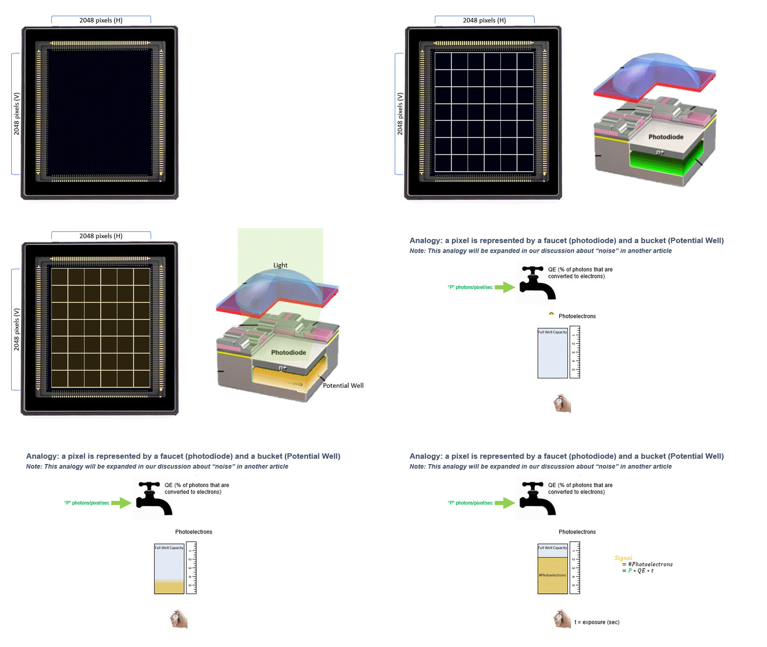
An “exposure” represents the time for which photoelectrons are collected in the bucket. A single image is formed by measuring the number of photoelectrons in each bucket and forming a digital representation of the entire array, which encodes the image as a 2-dimensional array of pixel values. The process is repeated to create a sequence of images: the collection of charge (referred to as exposure and integration), is followed by a readout of the data corresponding to number of photoelectrons collected at each photosite. The number of such image frames that are produced per second is referred to as the frame rate of the camera.
There are different types of imagers available, each with its own distinctive readout method. The following is an overview of three major types of imagers that are used in Scientific Imaging: Charge Coupled Devices (CCDs), Electron Multiplying CCDs (cmCCDs), and Complementary Metal Oxide Semiconductor Imagers (CMOS Imagers).
CCDs: Charge Coupled Devices
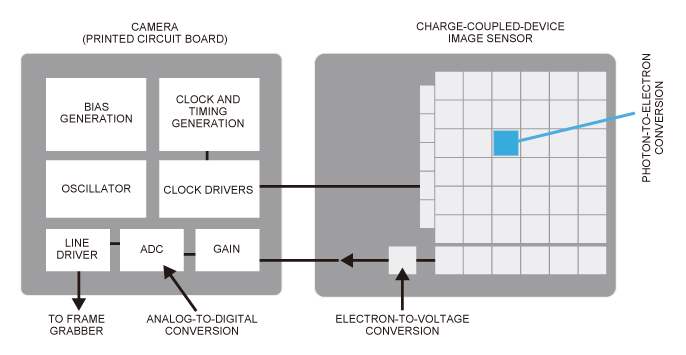
Figure 1: CCD Imager (shown schematically to describe its functionality)
Each pixel of the CCD image sensor (Figure 1) is composed of a photodiode and its corresponding potential well, which referring to our analogy, are the faucet and bucket for generating and collecting photoelectrons.
Light may be conceptualized as a flow of photons, a word used to describe discrete particles of light. A wavelength-dependent percentage of the photons that are incident on each pixel of the sensor is converted into electric charge (photoelectrons). This wavelength dependent conversion of light to photoelectrons is conveyed through the quantum efficiency (QE) specification of an imager.
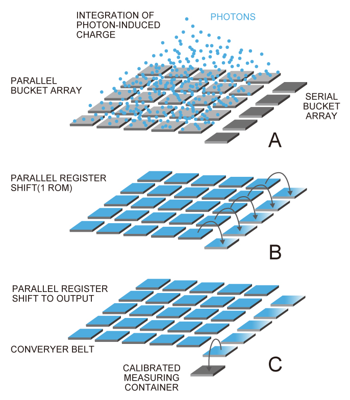
Figure 2: Photoelectrons are relayed down each row of pixels. A row of charges is loaded onto an output shift register and then clocked out serially.
Photoelectrons accumulate in each bucket until it is time for the pixels to be readout, when the photoelectrons are relayed from one bucket to the next down each row of pixels (Figure 2). The charge is gathered pixel-by-pixel—serially—into a container at the end of the relay. Once in the container, the photoelectrons (signal) are converted into voltage and processed into an image on the camera circuit board.
Even when the brightness of the incident light on a pixel is constant there is a temporal variation in its representation. This is referred to as noise, which will be detailed both qualitatively and quantitatively in other articles. One can conceive of this as the signal having to overcome noise to present a good representation of the light from the field-of-view of a camera. This gives rise to the use of the Signal-to-Noise Ratio (SNR) as a figure of merit to describe the quality of the generated images. Spatial non-uniformities in an image sensor can result in fixed-pattern noise, which can be noticed when viewing images on a display, or when analyzing images with the help of image processing algorithms.
In a CCD, the photoelectrons are converted into signal (voltage) at a common port. For this reason, the speed of image acquisition in a CCD is limited.
emCCDs: Electron Multiplying CCDs
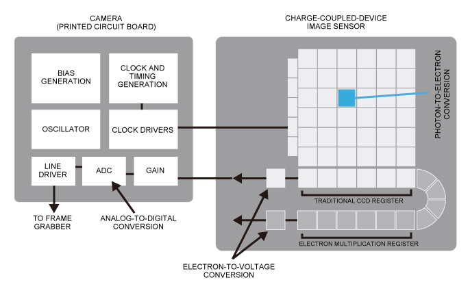
Figure 3: emCCD Imager (shown schematically to describe its functionality)
EM-CCD sensors (Figure 3) have an additional component, a multiplication register, that multiplies the photoelectrons prior to the readout of the sensor. If the gain of the multiplication register is, for example 10X, each photoelectron thus produces 10 electrons, increasing the signal value. This produces a brighter image since every pixel will be represented by a value that is 10X the original value. As in the case of a conventional CCD, the signal must overcome noise, the aggregate temporal uncertainty in the signal. The signal generated is larger than that of a conventional CCD as a result of electron multiplication. Therefore, one can expect a higher SNR in an emCCD than that of a conventional CCD without a multiplication gain register. That said, the multiplication process is probabilistic in nature and therefore introduces another source of temporal uncertainty. This noise is referred to as stochastic noise for the purposes of SNR estimations.
An emCCD is essentially a conventional CCD with a multiplication register. As in a conventional CCD, photoelectrons are converted into signal (voltage) at a common port. For this reason, the speed of image acquisition in an emCCD is limited.
CMOS Imagers
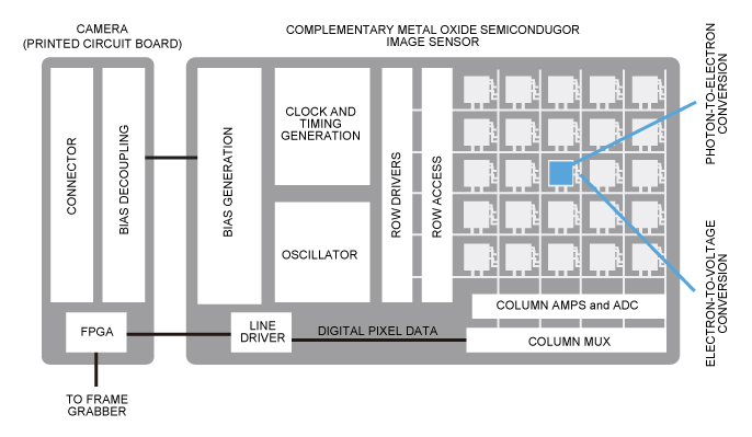
Figure 4: CMOS Imager (shown schematically to describe its functionality)
In contrast with CCD and EM-CCD sensors, each pixel of a CMOS image sensor (Figure 4) is composed of a photodiode-amplifier pair.
As in a CCD sensor, the photons incident on the pixels of a CMOS sensor are converted into photoelectrons, with conversion efficiency (QE) dependent on wavelength. But unlike a CCD sensor, photoelectrons are converted into voltage by each pixel’s photodiode-amplifier pair. The conversion to voltage in a CMOS sensor happens in parallel instead of the serial process described above in CCDs. For this reason, image acquisition can be much faster in CMOS sensors than in CCDs.
The optimized architecture of second-generation CMOS sensors combines high QE with fast frame rates and low noise—without the noise factor introduced by the multiplication register of EM-CCDs. This combination of capabilities translates into high speed, high-resolution biological images, even in low light situations.
References:
The next article is titled “The Photoelectric Effect in Image Sensors”. As the name implies, the Photoelectric Effect is a key concept with respect to understanding Image Sensors.

