The Photoelectric Effect
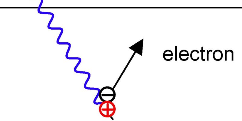
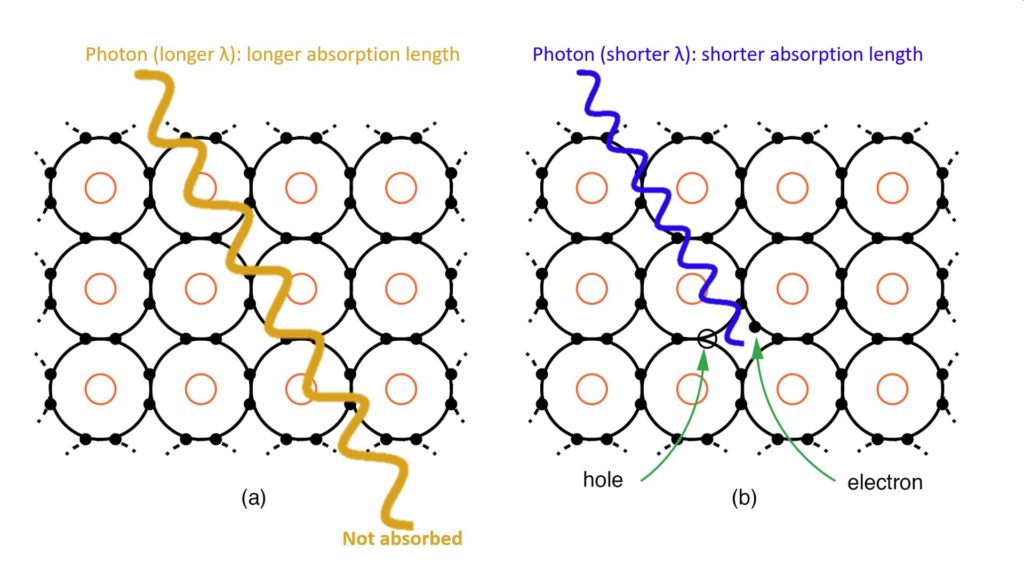
All image sensors rely on the Photoelectric Effect, which describes the interaction between light (photons) and materials (atoms). When an incident photon strikes a Silicon atom, an electron in the outer valence band of the Silicon atom may absorb the energy of the photon and transition to a higher energy level. This makes the electron mobile, leaving behind a “hole”, a term used to describe an atom that lacks an electron. An electron-hole pair is thus created. These electrons are referred to as photoelectrons since they are generated by photons.
Depletion regions are created in a pixel by selectively doping silicon with trace amounts of materials that cause a deficiency of electrons. This produces a positively charged region in each pixel which attracts photoelectrons while repelling holes.
Photoelectrons are collected in the static depletion area within each pixel. Holes are repelled away from the depletion region, thus preventing their recombination with the photoelectrons.
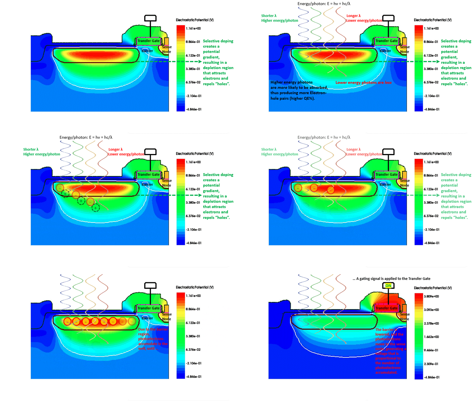
Image Formation
Photoelectrons that are generated by the Photoelectric Effect (described above) can be collected by establishing an electric field within the substrate of the imager. Such an electric field is set up in the imager using dopants to make a potential well a.k.a depletion region. Image sensors form an image by collecting and measuring the number of photoelectrons generated in the depletion region of a pixel, the smallest spatial unit on the imaging surface of an image sensor.
An image sensor may be a one-dimensional or two-dimensional array, constituting a matrix of pixels. Since the number of photoelectrons is proportional to the number of photons that were incident on the pixel, the matrix of values representing the photoelectrons in each pixel forms a one-dimensional or two-dimensional image frame. A single frame or a temporal sequence of such frames at a suitably high frame-rate can be displayed on a monitor to show a two dimensional image and/or to show movement or other changes in the field of view.
Thermally generated electrons: Dark Current
Electrons may also be thermally excited into the conduction band within the substrate, and if this event occurs near or within the depletion region, the electrons created in this process may also be collected in the depletion region along with the photoelectrons. Thermally generated electrons collected in this manner are indistinguishable from photoelectrons. These electrons are generated even when there is no light on a pixel. The flow of thermally generated electrons is often referred to as dark current – an unwanted, strongly temperature-dependent flow that is a result of lattice defects or metal impurities in the silicon lattice of the imager. An impurity or lattice defect creates an alternative pathway for electrons excited by heat within the imager to leave the valence band and reach the conduction band. In effect, less energy is needed to excite these electrons.
Once in the conduction band thermally generated electrons can be collected in the depletion region, partially filling the potential well. Dark current is primarily a problem when there is a low level of light and the number of thermally generated dark electrons is close to the number of photoelectrons. Cooling an image sensor reduces the dark current.
The temporal variation in the number of thermally generated electrons results in dark-shot-noise, which is discussed in the article on Dark Noise. In addition, dark current varies from pixel to pixel on the imager due to variations in defects and impurities, creating a fixed pattern referred to as hot pixels. These may be observed as a collection of bright points in an otherwise dark image that is taken at long exposures when no light is incident on the imager. Exceedingly hot pixels, pixels that show a much larger dark current than their neighbors, can be visually apparent even at shorter exposures.
The Optical Properties of Silicon
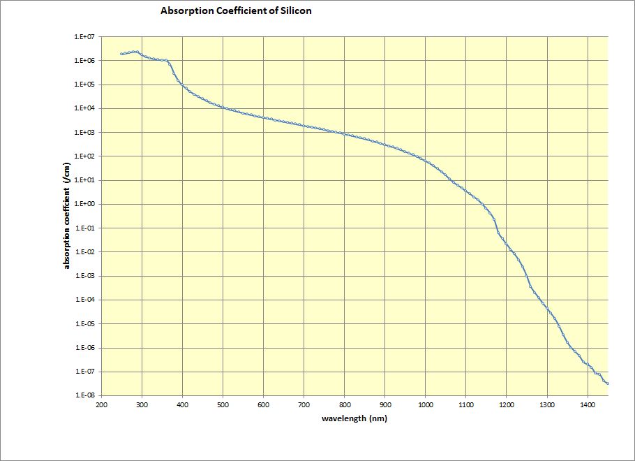
Absorption coefficient of silicon in cm-1 as a function of the wavelength. The data is graphed on a log scale. The drop in absorption at the band gap (around 1100 nm) is sharper than might first appear.
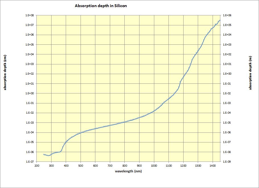
The absorption depth is the inverse of the absorption coefficient. An absorption depth of, for example, 1 um means that the light intensity has fallen to 36% (1/e) of its original value. From www.pveducation.org
The quantum efficiency (QE) of an imager is defined as the number of electron-hole pairs created and successfully read out for each incoming photon. It is a function of the material used (e.g. silicon) as well as any structures that exist in the optical path of the pixel, for example, faceplates, micro-lenses, gate structures, etc. It is typically expressed as a percentage, representing the probability that a photon of a particular wavelength will be detected.
As shown in the interactive graph below, the QE of a pco.panda 4.2 bi non-cooled, Back Illuminated sCMOS camera at 550nm is estimated to be 92%. This means that out of every 100 incident photons at λ = 550nm, 92 are likely to be detected by the imager.
The following table shows a selection of cameras with high QE, Back Illuminated sCMOS imagers, with their salient specifications:
** Peak QE is shown for monochrome versions of each camera series (see QE Curves above). Max frame rate is displayed as max frame rate at full resolution.
The Upper Limit of Spectral Response for Silicon
Silicon has a bandgap energy of Eg = 1.12eV
From Planck’s equation: Wavelength λ = (hc)/Eg
λ = (4.135×10⁻¹⁵ eV.s x 3×10⁸ m/s)/1.12 eV = 1110 nm
This means that photons corresponding to infra-red wavelengths longer than 1110nm do not have enough energy to energize an electron up from the valence band to the conduction band; thus silicon is transparent above 1100nm.
Photons are absorbed in the depletion region of the imager. The probability of absorption for photons with longer (red) wavelengths is lower, and this limits the sensitivity of Silicon imagers at these wavelengths. As mentioned above, the bandgap energy of Silicon [Eg = 1.12eV] sets an upper limit of 1100nm for silicon-based devices. Applications requiring responsivity above 1100nm typically use detectors made with InGaAs and other materials.
Spectral responsivity is an estimate of the number of photoelectrons that are generated by a unit of radiant energy (1 nJ/cm2). It conveys similar information as the Quantum Efficiency, but allows us to conceptualize the conversion of light to photoelectrons in radiometric units. This can be useful in, for example, estimating the response of a camera to laser illumination at different energy levels and/or wavelength.
References:
- A Review of the Pinned Photodiode for CCD and CMOS Image Sensors
- M. A. Green and Keevers, M. J., “Optical properties of intrinsic silicon at 300 K”, Progress in Photovoltaics: Research and Applications, vol. 3, pp. 189 – 192, 1995.
- 2.M. A. Green, “Self-consistent optical parameters of intrinsic silicon at 300 K including temperature coefficients”, Solar Energy Materials and Solar Cells, vol. 92, pp. 1305–1310, 2008.

