Images taken under ultraviolet illumination can serve a number of scientific, medical, industrial or artistic purposes. In addition to the inspection of optical and semiconductor materials, these cameras may be used to reveal deterioration of art works or structures not apparent under visible light. Diagnostic medical imaging may be used to detect certain skin disorders or as evidence of injury. Ultraviolet imaging of archaeological sites may reveal artifacts or patterns not otherwise visible.
Ultraviolet sCMOS cameras are optimized for acquiring images from the near ultraviolet (NUV) spectrum [200nm – 380nm] under low light conditions. Since the diffraction limit is proportional to the wavelength of light, one can resolve smaller features in the UV than at higher wavelengths (all else being equal). For this reason, UV microscopy is often used when it is critical to image small features, for example in semiconductor wafers. When used with suitable UV microscope optics, these cameras can help resolve much smaller features than otherwise possible.
The following cameras combine high QE in the UV region, relatively large pixels for optimal photon collection and the low read noise that characterizes sCMOS cameras. Non-cooled cameras are a good choice for applications in which relatively short exposures are sufficient – while TE-cooled camera is recommended when long exposures are preferred.
UV sCMOS Cameras
| Camera Series | TE cooled | #Mpix | Estimated QE (%) at λ = 240nm | min. read noise [e-] RMS | Number of pixels | Pixel size (µm) | Image Sensor Diagonal (mm) | Shutter type | Max frame rate at full resolution (fps) | Interface |
|---|---|---|---|---|---|---|---|---|---|---|
| Dhyana 95V2-UV | Yes | 4.2 | 79 | 1.7 | 2048 x 2048 | 11 x 11 | 31.9 | RS | 48 | USB3.0 | CameraLink |
| pco.edge 4.2 bi uv | Yes | 4.2 | 60 | 1.8 | 1.1 (Low Light Mode) | 2048 x 2048 | 6.5 x 6.5 | 18.8 | RS | 40 | USB 3.1 Gen 1 |
| pco.panda 4.2 bi uv | No | 4.2 | 54 | 1.8 | 1.1 (Low Light Mode) | 2048 x 2048 | 6.5 x 6.5 | 18.8 | RS | 40 | USB 3.1 Gen 1 |
* QE at λ = 240nm is shown for each camera series.
** The Max Frame Rate shown in the above table for each camera is the maximum frame rate achievable at full-frame readout.
QE Curves
The following is an interactive plot of the QE curves for cameras based on BSI sCMOS imagers. They are shown on one graph so that it is possible to make comparisons. The following interactive features of this graph can be helpful:
- Use your mouse to hover over the legend of a particular camera to see it highlighted in the graph below.
- Click on the legend of a camera to turn on or off its plot.
- Use your mouse to read QE data for all displayed imagers at the wavelengths of interest.
- Right-click and drag to zoom-in along the X-axis to expand the view for a desired range of wavelength.
- To pan left or right within a zoomed-in view, hold down the Shift key and use your mouse.
- To revert from the zoomed-in view to the normal view, click on the “Reset zoom” button that is displayed at the top-RHS of the graph.
Estimated Signal-to-Noise Ratios
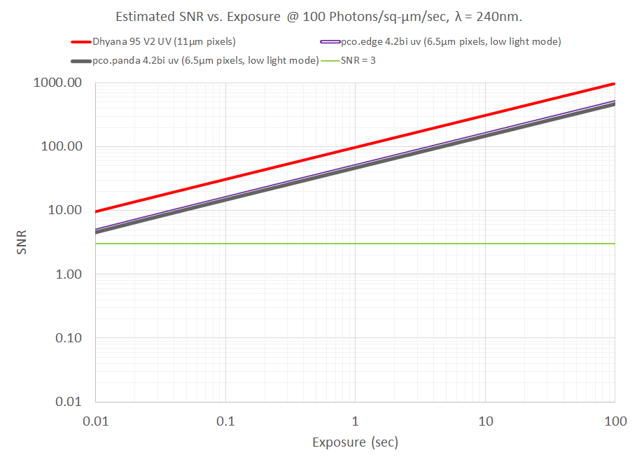
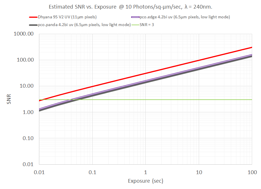
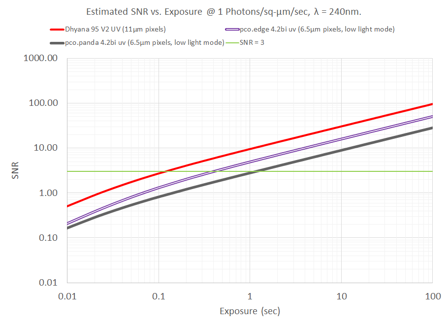
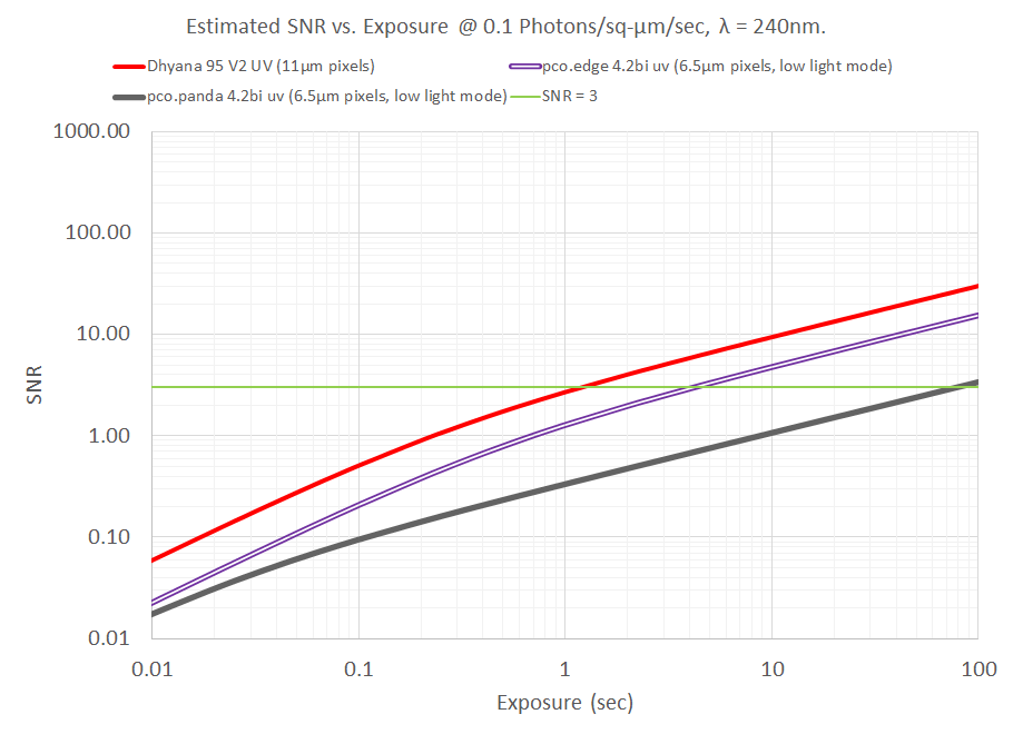
Using the method that was described in the article “Estimating Camera Performance” we show the plot of the estimated SNR vs Exposure at different levels of Photon Flux density. For this example, we have chosen QE values at λ = 240nm, a wavelength of interest in many UV imaging applications. These graphs are provided for references purposes only – no guarantees of performance are implied.
In the following sequence, the Photon Flux Density is reduced by an order of magnitude from one graph to the next. The Dhyana 95 V2 UV camera outperforms the other two cameras in all cases because it has 11μm pixels while the other two cameras have 6.5μm pixels. The TE-cooled Dhyana 95 V2 UV camera thus has nearly 2.9x the pixel area of a camera with 6.5μm pixels and is recommended for UV imaging applications which can benefit from its large (31.9mm) imager diagonal.
The first two graphs represents instances of relatively high Photon Flux Densities of 100 Photons/sq-μm/sec. and 10 Photons/sq-μm/sec. In these cases all three cameras perform very well, and users would be well-advised to select the non-cooled pco.panda 4.2 bi uv due to its lower price.


In the third graph of the above sequence, the Photon Flux Density is lowered to 1 Photon/sq-μm/sec. The divergence between the estimated performance of the cooled and the non-cooled cameras quite noticeable: the non-cooled cameras is dark-shot-noise limited. A TE-cooled camera is highly recommended. The non-cooled pco.panda 4.2 bi uv would theoretically achieve an SNR=3 image at an exposure of about 1sec (which is above its maximum exposure of 500ms). The cooled pco.edge 4.2 bi uv camera achieves an SNR=3 image at an exposure of about 400ms. The TE-cooled Dhyana 95 V2 UV achieves an SNR=3 at an exposure of about 110ms.
In the last graph of the above sequence, the Photon Flux Density is at an extremely low value of 0.1 Photons/sq-μm/sec. The cooled pco.edge 4.2 bi uv camera achieves an SNR=3 image at an exposure of about 4sec. The TE-cooled Dhyana 95 V2 UV is estimated to achieve an SNR=3 at an exposure of about 1.1s.
For UV Microscope users
The following table shows the estimated performance of the following UV sCMOS cameras when they are used with UV microscopes:
- pco.panda 4.2 bi uv [non-cooled, 4.2MPix, sCMOS camera with UV window]
- pco.edge 4.2 bi uv [cooled, 4.2MPix, sCMOS camera with UV window]
The specifications of commercially available UV objectives are used in this table. This table is provided for references purposes only – no guarantees of performance are implied.
| Camera Parameters | ||||||||
| Optical Format | #Megapixels | #H pixels | #V pixels | Pixel size (μm) | H size (mm) | V size (mm) | Diagonal (mm) | |
| 18.8mm < 4/3" | 4.2 | 2048 | 2048 | 6.5 | 13.31 | 13.31 | 18.83 | |
| Commercially Available NUV Objectives | ||||||||
| Objective: Mag/NA | 10X\0.25NA | 20X\0.4NA | 20X\0.36NA | 50X\0.65NA | 50X\0.42NA | 50X\0.41NA | 80X\0.55NA | 100X\0.5NA |
| Min. feature size (um) | 0.65 | 0.41 | 0.45 | 0.25 | 0.39 | 0.40 | 0.30 | 0.32 |
| Max pix size (um) | 3.25 | 4.10 | 4.50 | 6.25 | 9.75 | 10.00 | 12.00 | 16.00 |
| FN (mm) | 22 | 22 | 22 | 22 | 22 | 22 | 22 | 22 |
| WD (mm) | 20 | 16.96 | 15 | 9.76 | 14.76 | 12 | 10 | 11.03 |
| NA | 0.25 | 0.4 | 0.36 | 0.65 | 0.42 | 0.41 | 0.55 | 0.5 |
| Magnification | 10 | 20 | 20 | 50 | 50 | 50 | 80 | 100 |
| Estimated Performance of Camera and Objective Combinations @ λ = 266nm | ||||||||
| (*) Limiting Resolution (µm) | 1.3 | 0.65 | 0.65 | 0.26 | 0.39 | 0.4 | 0.3 | 0.32 |
| Vignetting? | No | No | No | No | No | No | No | No |
| FOV (H x V) mm | 1.33 x 1.33 | 0.67 x 0.67 | 0.67 x 0.67 | 0.27 x 0.27 | 0.27 x 0.27 | 0.27 x 0.27 | 0.17 x 0.17 | 0.13 x 0.13 |
| FOV (diagonal) mm | 1.88 | 0.94 | 0.94 | 0.38 | 0.38 | 0.38 | 0.24 | 0.19 |
| Please contact our imaging experts for assistance in selecting a camera & objective combination that fulfils your FOV & resolution requirements at application-specific wavelengths. | ||||||||
| 1) The minimum feature size is estimated using the Rayleigh Criteria at λ = 266nm; it can be re-calculated for other wavelengths. R = 1.22*λ/(2NA) | ||||||||
| 2) The maximum pixel size is estimated by applying the Nyquist criteria to the minimum feature size as it appears on the imager plane. Maximum pixel size = R*magnification/2 | ||||||||
| 3) Camera and Objective combinations which meet the Nyquist criteria and are therefore diffraction limited are indicated by showing the Limiting Resolution in green font. (*) | ||||||||
| 4) Values for Working Distance (WD) and Field Number (FN) are shown for reference only. Actual values may vary. | ||||||||
| 5) Vignetting, a darkening of the image at the corners, may be observed if the Imager Diagonal is larger than the Field Number of the Objective. | ||||||||
Please contact us for assistance in the process of matching the right imager with the requirements of your application. As detailed in the list of prioritized criteria for Scientific Camera selection, it is important to prioritize photonics performance as the first step in the camera selection process.

